Solder Paste Inspection (SPI) Technology in PCBA Assembly
Solder Paste Inspection (SPI) is one of the most critical quality control steps in a Surface Mount Technology (SMT) assembly line. Installed immediately after the stencil printing stage, SPI is an automated, non-contact measurement technology that verifies the volume, shape, and position of the solder paste deposits before component placement and reflow soldering. This early intervention is essential because approximately 60% to 70% of all PCBA defects originate from poor solder paste printing.
The Imperative of 3D Measurement
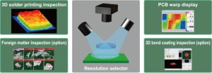
Modern SPI systems operate almost exclusively using 3D measurement technology to accurately quantify the paste deposit. Like 3D AOI, the technology typically employs structured light projection and triangulation principles:
- Light Projection: A precisely controlled pattern of light (e.g., moiré fringes or structured stripes) is projected onto the solder paste deposit.
- Image Capture: A camera captures the image of the deformed light pattern. The height and volume of the paste cause the projected lines to shift or curve.
- Measurement: Software analyzes the degree of deformation to accurately calculate the three-dimensional characteristics of the paste deposit:
- Volume: The total amount of solder paste, directly correlating to the resulting solder joint strength.
- Height: The maximum height of the deposit, ensuring consistency across the board.
- Area: The footprint of the deposit, confirming correct alignment with the PCB pad.
This precise data is far superior to 2D inspection, which can only infer volume based on light reflectivity, often leading to high false-call rates.
Key Inspection Parameters and Defect Detection
SPI systems measure a comprehensive set of parameters against pre-programmed specifications derived from the stencil design and component requirements:
| Parameter | Measurement Goal | Associated Printing Defects |
| Volume | Target volume ±20% | Insufficient Paste (leads to open circuits), Excess Paste (leads to bridging). |
| Area | Alignment with pad ±50μm | Misalignment (offset printing), Smeared Print (poor squeegee control). |
| Height | Consistency across all pads | Uneven Height (poor stencil release or clogging). |
| Shape/Bridging | Paste separation | Bridging/Shorts (excess paste connecting adjacent pads). |
Detecting these defects at the printing stage is critical because the paste can be easily wiped off and the board reprinted. Attempting to fix these defects after reflow soldering is costly, time-consuming, and can damage the PCBA.
Process Optimization and Feedback Loop
The greatest value of SPI lies in its ability to provide real-time, quantifiable feedback to the stencil printer. This forms a closed-loop control system for process optimization:
- If the SPI data indicates a systematic shift in paste volume (e.g., all deposits are too low), the system can automatically signal the printer to adjust parameters like squeegee pressure or print speed.
- If contamination or clogging is detected on the stencil, the SPI system can alert the operator to initiate an automated under-stencil cleaning cycle.
By establishing the Solder Paste Volume Standard Deviation as a key process indicator, factories use SPI data to maintain optimal printing quality, maximizing the First Pass Yield (FPY) of the entire SMT line and reinforcing the principles of intelligent manufacturing in a modern PCBA factory.
P&C Enterprise Solutions (PCES) is a trusted OEM/ODM electronics manufacturer based in Vietnam. Our electronic components and embedded solutions have been delivered to customers across Europe, Asia, and the Middle East, supporting a wide range of industries including audio systems, GPS devices, elevators, lighting, and automation. With strong in-house capabilities in product design, hardware, firmware, and mass production, we provide fully customized solutions tailored to your specific project requirements.
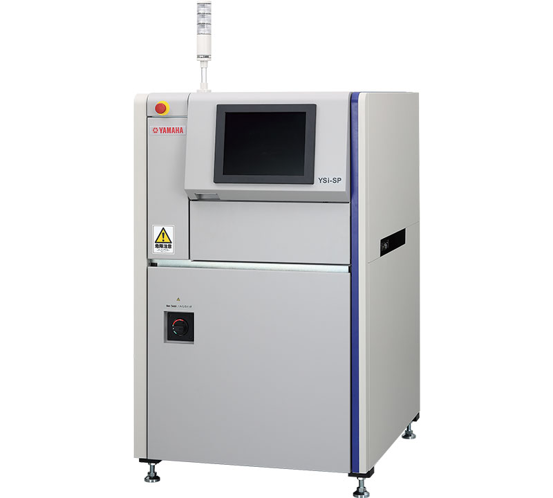
P&C factory is equipped with Solder Paste Inspection (SPI) machine model YSi-SP from Yamaha. P&C ensures that product quality commitment always meets the most stringent standards, meeting high-end product requirements.
Source: PCES