3D Automated Optical Inspection (AOI) Technology in PCBA
3D Automated Optical Inspection (AOI) has emerged as a crucial quality control technology in modern Printed Circuit Board Assembly (PCBA) factories, significantly surpassing the capabilities of traditional 2D systems. It provides a non-contact, high-speed method for verifying the quality of component placement and solder joints by capturing and analyzing three-dimensional height data of the assembled board.
The Working Principle: Capturing the Z-Axis
Unlike 2D AOI, which relies solely on top-down image comparison (X-Y plane) and contrast analysis, 3D AOI uses advanced optical techniques to generate a full topographical map of the PCBA.
- Structured Light Projection: The most common method involves projecting a known pattern of light (like stripes or grids) onto the surface of the PCB.
- Multi-Camera Acquisition: Multiple high-resolution cameras, positioned at various angles, capture the image of the PCB. As the light pattern strikes the components and solder joints, the pattern deforms.
- Triangulation and Reconstruction: The system’s software analyzes the distortion of the projected light pattern using triangulation principles to calculate the precise height, shape, and volume (Z-axis) of every feature on the board. This data is then reconstructed into a detailed 3D model.
By combining the 2D color images with the precise 3D height data, the system can accurately measure and inspect complex features.
Enhanced Defect Detection Capabilities
The ability to measure the Z-dimension allows 3D AOI to detect defects that are invisible or ambiguous to 2D systems, dramatically reducing false calls (false positives) and improving first-pass yield.
| Defect Type | 2D AOI Capability | 3D AOI Capability |
| Solder Volume | Inferential (based on reflection/color) | Direct Measurement (measures height and volume) |
| Lifted Leads | Difficult/Missed (shadows can hide gap) | Direct Detection (measures component coplanarity) |
| Component Tilt | Difficult (based on distorted outline) | Direct Measurement (calculates tilt angle) |
| Bridging/Shorts | High contrast required | Direct Measurement (checks separation distance and height) |
Specifically for solder joints, 3D AOI can verify essential parameters like solder fillet shape, volume, and maximum height, ensuring compliance with strict industry standards (e.g., IPC-A-610). This is critical for modern high-density interconnect (HDI) boards and fine-pitch components where a slight deviation in solder volume can lead to field failure.
By integrating seamlessly into the Surface Mount Technology (SMT) line, typically post-reflow, 3D AOI provides valuable, quantifiable process data that allows manufacturers to proactively adjust upstream processes, fulfilling the promise of Industry 4.0 quality control.
P&C Enterprise Solutions (PCES) is a trusted OEM/ODM electronics manufacturer based in Vietnam. Our electronic components and embedded solutions have been delivered to customers across Europe, Asia, and the Middle East, supporting a wide range of industries including audio systems, GPS devices, elevators, lighting, and automation. With strong in-house capabilities in product design, hardware, firmware, and mass production, we provide fully customized solutions tailored to your specific project requirements.
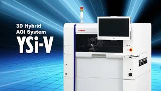
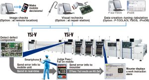
P&C factory is equipped with 3D Automated Optical Inspection (AOI) machine model YSi-V from Yamaha. P&C ensures that product quality commitment always meets the most stringent standards, meeting high-end product requirements.
Source: PCES