Wave Soldering Technology in PCBA Electronics Assembly
Wave soldering remains a cornerstone technology in the Printed Circuit Board Assembly (PCBA) industry, particularly for through-hole components and for the selective soldering of mixed-technology boards (Surface Mount Technology and Through-Hole Technology components). While reflow soldering dominates for pure SMT assemblies, wave soldering offers distinct advantages for high-reliability, high-mechanical-strength through-hole connections.
The Principle of Operation
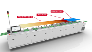
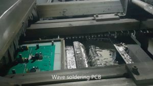
At its core, wave soldering involves passing a PCBA over a standing wave of molten solder. This process ensures that all exposed metallic pads and component leads on the underside of the board are wetted and subsequently soldered. The entire operation is a meticulously controlled sequence of four main stages: flux application, preheating, actual soldering, and cooling.
1. Flux Application
The first stage involves applying a uniform layer of flux to the underside of the PCBA. Flux serves several critical functions:
- Cleaning: It removes oxides and other contaminants from the metallic surfaces (pads and component leads) that would otherwise prevent proper wetting by the molten solder.
- Wetting Promotion: It lowers the surface tension of the molten solder, allowing it to flow more readily and create a robust metallurgical bond.
- Heat Transfer: It aids in transferring heat from the preheating stage to the board.
Common application methods include spray fluxing, foam fluxing, and drop-jet fluxing. The choice depends on board complexity and flux type.
2. Preheating
After fluxing, the PCBA enters the preheat zone. This stage is crucial for several reasons:
- Solvent Evaporation: It evaporates the volatile solvents in the flux, preventing spattering and voids during the soldering phase.
- Thermal Shock Mitigation: It gradually elevates the board’s temperature, minimizing thermal shock when it contacts the much hotter molten solder wave.
- Flux Activation: It brings the board and flux to the optimal activation temperature, where the flux’s cleaning action is most effective.
Preheating is typically achieved using infrared heaters, hot air convection, or a combination of both. The preheat profile (temperature over time) is critical and must be carefully tuned to the board and component characteristics.
3. Wave Soldering
This is the central stage where the electrical and mechanical connections are formed. The PCBA travels over one or more waves of molten solder, typically an alloy of tin, lead (in older systems or specific applications), and increasingly, lead-free alloys like SAC (Tin-Silver-Copper).
There are generally two types of solder waves:
- Turbulent Wave (Chip Wave): A high-pressure, narrow wave used to ensure solder penetrates small clearances and removes any trapped gases from beneath SMT components (if soldering mixed technology boards).
- Laminar Wave (Main Wave): A smoother, broader wave that creates the final solder joints. Its calm surface tension promotes excellent wetting and allows excess solder to drain away, preventing bridging.
The dwell time (how long the board is in contact with the solder wave) and wave height are critical parameters adjusted to achieve optimal solder joint formation without defects like shorts or insufficient fill.
4. Cooling
Immediately after exiting the solder wave, the PCBA enters the cooling zone. Controlled cooling ensures the solder solidifies uniformly, preventing thermal stress on components and minimizing grain structure issues in the solder joints. Rapid cooling can lead to stress and micro-fractures, while excessively slow cooling can result in grainy solder joints. Air convection systems are commonly used for this stage.
Challenges and Considerations
While robust, wave soldering presents challenges such as:
- Bridging: Unwanted solder connections between adjacent pads.
- Misses/Non-wetting: Incomplete solder joints due to insufficient wetting.
- Voids: Bubbles or empty spaces within the solder joint, often caused by trapped flux solvents.
- Dross Formation: Oxidation of molten solder, which can lead to defects and material waste.
Modern wave soldering machines incorporate advanced controls, inert nitrogen atmospheres (to reduce dross and improve wetting), and sophisticated wave shaping nozzles to mitigate these issues and ensure high-quality, reliable solder joints, making it an indispensable process in many electronics manufacturing facilities.
P&C Enterprise Solutions (PCES) is a trusted OEM/ODM electronics manufacturer based in Vietnam. Our electronic components and embedded solutions have been delivered to customers across Europe, Asia, and the Middle East, supporting a wide range of industries including audio systems, GPS devices, elevators, lighting, and automation. With strong in-house capabilities in product design, hardware, firmware, and mass production, we provide fully customized solutions tailored to your specific project requirements.
PCES